Achilles – Multilayer Cushions
The cushions are the main protection placed inside the wafer carriers and absorbing external chocks and internal moves of the wafers stack. They are compatible with 4“, 5“, 6“, 8“ and 12“ wafers, and exist with different thicknesses: 3mm…
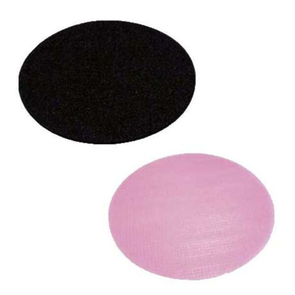
The cushions are the main protection placed inside the wafer carriers and absorbing external chocks and internal moves of the wafers stack. They are compatible with 4“, 5“, 6“, 8“ and 12“ wafers, and exist with different thicknesses: 3mm, 5mm and 6mm.
Their multi-layer structure improves their mechanical performances and offers a high purity grade. One thick PE core is covered with PE films on both sides.